


순차회로
SR Latch (1 bit 짜리 메모리 사용 가능)

SR = 00 -> Qnext = Qcurrent - hold
SR = 10 -> Qnext = 1 - set
SR = 01 -> Qnext = 0 -reset
SR = 11 -> 모순이 생김

S'R' Latch

S'R' Latch with control input

D Latch
:based on S'R' Latch


Latch의 실사용

Latch의 timing issue problem -> clocks and flip-flops 로 해결

clock : synchronize our latches with the ALU (enable)
when clock = 1 , the latches will be enabled for writing.

flip flop : enable a latch for just an instant (enable just once)
D flip flop ( D Latch + SR Latch )
- D flip flop's control input C enables either the D latch or the SR latch, but not both.
- when C=0
- master latch is enabled, and master's output changes whenever D changes
- slave latch is disabled, just maintains the flip flop's current state
- when C=1
- master is disabled, its output will be the last D input value's output
- slave is enabled

Direct input (D flip flop에 적용)


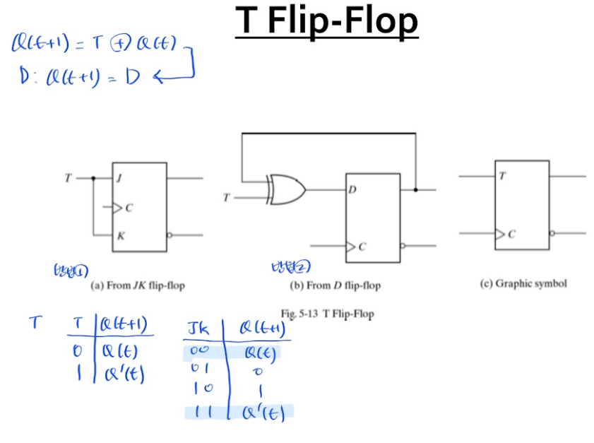
JK flip flop , T flip flop

characteristic tabels (특성표)
: Q(t) -> Q(t+1) 현재 입력으로 다음번 출력을 나타내기

characteristic equations (특성 방정식)

JK flip flop 회로

T flip fop
JK flip flop timing diagram - 강의 자료 참고 (귀찮아서 안 붙임)
순차회로 분석 -> 1. state table (상태표)
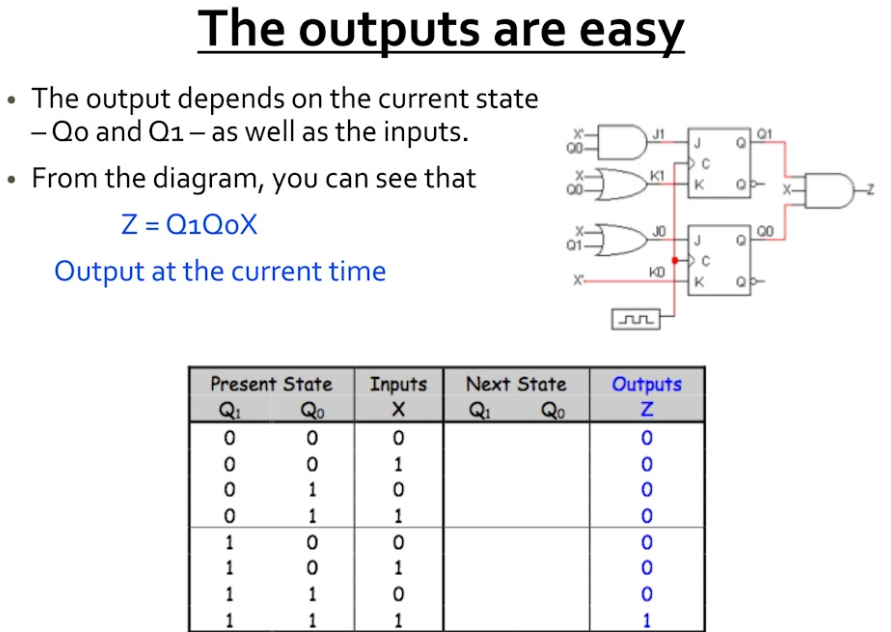
next state 구하기
step1 : flip flop input equations (find boolean expressions for the flip flop inputs)
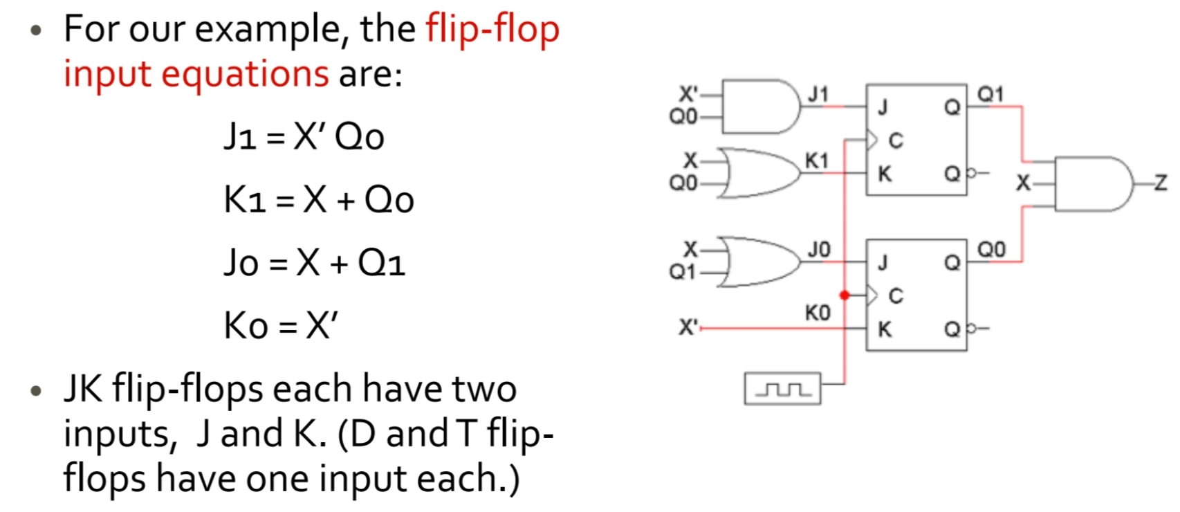
step2 : flip flop input values (real input values)

step3 : find the next state (using flip flop characteristic tables or equations)

결과:

순차회로 분석 -> 2. state diagram (상태선도)
state table (상태표)를 만든 다음 state diagram (상태 선도)로 만들 수도 있음


회로도 분석 = state table or state diagram 만들면 됨.
특정 순차회로 설계(분석의 역방향)>
- Mealy state machine
- output depends on both present state and current input
- updated without change in clock
- Moore state machine
- output depends only on present state
- updated at the clock edge
state reduction -> reduce the number of flip-flops

+ state assignment
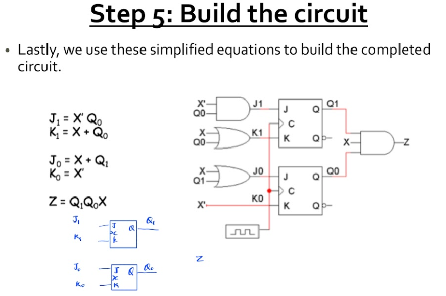
순차회로 설계
step1 : make a state table (state diagram -> state table)
step2 : assign binary codes to each states (if have n states, binary codes will have at least log2 n digits)
step3 : finding flip-flop input values
step4 : flip flop input euqations 과 output equations 을 찾기
step5 : build circuit
(예제) - sequence recognizers
: our example will detect the bit pattern '1001'

step1 : make state table (state diagram -> state table)

step2 : assign binary codes to each state
A with Q1Q2 = 00 , B with Q1Q2 = 01 , C = 10 , D = 11
step3 : finding flip flop input values
JK or D or T 먼저 결정 , 여기표 결정
*여기표(excitation table)

여기표 사용해서 flip flop input values 채우기

step4 : find equations for the FF inputs and output

step5: build circuit
timing diagram

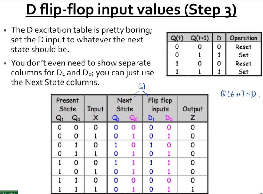
위 예제에 D flip flop 사용
step3 : D flip flop input values
step4 : equations

step5 : circuit

'cs > 컴퓨터회로' 카테고리의 다른 글
| [컴퓨터회로] Memory and Programmable logic A,B (0) | 2023.11.29 |
|---|---|
| [컴퓨터회로] Registers and counter -part A,B (2) | 2023.11.24 |
| [컴퓨터회로] Ch3. GATE level Minimization (1) | 2023.10.02 |
| [컴퓨터회로]Chap2. Boolean algegra and logic gates (0) | 2023.09.23 |
| [컴퓨터회로 : chap1. digital systems and binary numbers] (0) | 2023.09.07 |